|
No.2/Year 1 - February 2007 |
| |
CHARACTERIZATION FACILITIES OFFER BY IMT-BUCHAREST - Microphysical characterization
 ATOMIC FORCE MICROSCOPE (AFM): ATOMIC FORCE MICROSCOPE (AFM):
- Provides 3D measurements of surface morphology with nanometric resolution.
- Investigations are done under ambient conditions.
- Generally requires no sample preparation or coating.
- Admits both conductive and nonconductive samples.
- Imaging forces are typically three orders of magnitude smaller than for stylus profilometry (pN-nN)
- maximum scan area: 20 x 20 microns
- maximum measurable roughness: 5 microns
- resolution: x, y: typical 20 nm; vertical: 2 nm
|
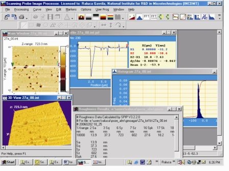 |
Equipment: Home-built AFM at Twente University.
In the very next future it will be replaced by a complex SPM equipment provided with additional operating modes suitable for biologic samples and nontopographic material properties.
Contact: Phys. Raluca Gavrila, e-mail: [email protected];
|
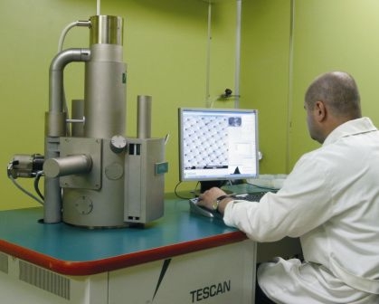
SCANNING ELECTRON MICROSCOPE (SEM)
- digital image acquisition.
- network operations, remote control and diagnostics (via TCP/IP)
- possibility of examination of non-conducting, water containing specimens in their natural state at low vacuum conditions in microscope chamber:
- Accelerating voltage 200V-30kV
- Rezolution 3nm
- Magnification 6 X - 1.000.000 X
- Maximum image size 16 mega pixeli;
|
|
Equipment: SEM - TESCAN VEGA II LMU.
has been up-graded with an EDX equipment for qualitative and quantitative
measurements.
Contact: Phys. Adrian Dinescu, e-mail: [email protected];
|
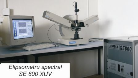
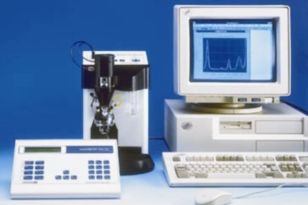
SPECTROSCOPIC Ellipsometer (SE 800 XUV)
- Analysis and characterization equipment for the nanometric thin films, interfaces, multi layer structures from different materials/dielectrics, conductive oxides, polymers, semiconductors. Measuring the index of refraction (n) and the extinction coefficient (k) for a single layer permits one to determine the material composition and
modeling of optical performance.
- Spectral range (240-750) nm, with variable dimension of the spot from 4 to 0.1 mm and also of the angle (from 0 to 90 degree) with 0.01 degree accuracy.
- Operating software, SPECRARAY II /WINDOWS, enables the fast data acquisition and analysis of the measured data.
- The modular construction has the possibility of extension to IR range (until 2500 nm) and 2D- and 3D- representation of data.
Contact: PhD. Munizer Purica, e-mail: [email protected];
|
|
| |
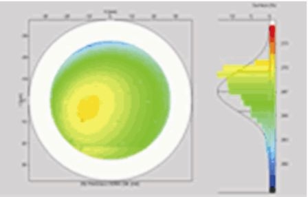
2D contour plot using
SENTECH's advanced
mapping software |
|
| |
|
Characterization equipments available in NANOBIOLAB
technological area (clean room) in MINATECH-RO
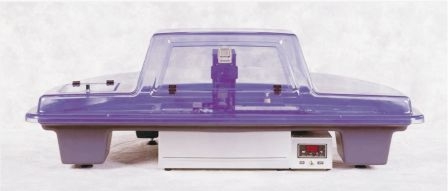
- Nano-Plotter "GeneMachines OmniGrid Micro": allowing bio-chips
development; dispersing of adhesives and
liquid crystals; analysis of adherent cells or
tissue slices, for nanobiotechnology projects as lab on chip, biochips.
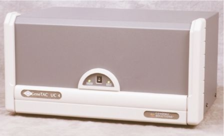
- "GeneTAC UC4 Microarray Scanner": this equipment is used for reading the chips, acting as a pair of the nano-plotter, for DNA detecting and deposition.Contact: PhD. Carmen Moldovan, e-mail: [email protected];
|
|
Nano-Plotter GeneMachines OmniGrid Micro |
GeneTAC UC4 Microarray Scanner |
|
| |
|
Characterization equipments available in Nanotechnologies Laboratory
- Trace Lab-VoltaLab 50 (PST050&Volta Master 4) - for electrochemical
measurements;
- Low noise preamplifier w.RS232 with interface, for electrical measurements;
- Heating/ Cooling testing system on wafers, for electrical measurements and wafer testing;
- AMMT: wet etching system for 4' silicon wafers with dedicated software,
potentiostat MC, silicon etching power supply;
- Transmission- reflexion- fluorescence microscope with images acquisition and measurement system;
Contact: PhD. Irina Kleps, e-mail: [email protected];
|
Keithley model 6487-picoammeter/
voltage source- 2004, used for electrical measurements; |
| |
UV- VIS-NIR Spectrophotometer
The spectrophotometer SPECORD M42 with double spot and (200 � 900)nm spectral range contains modules for transmittance and reflectance
measurements and enables data acquisition by a PC in order to processing of the measured data with specific software's.
- Optical characterization of thin films by recording the transmission and absorption spectra for transparent samples and for solutions with +/- 0.3 nm
precision in wavelength
- The reflectivity characterization of the texturized and porosified surfaces,
- The processing of T and R spectra leads to the knowledge of material properties: the absorption coefficient and the bandgap for the semiconductor
and dielectric films.
Raman spectrometer by IMT through a P-CONFORM project - IV module CEEX Competition - with the financing starting 2006 will enable the extension of possibilities for the structural characterization using optical methods at molecular and nanometric scale.nivel nanometric si molecular.
Contact: PhD. Munizer Purica, e-mail: [email protected]; |
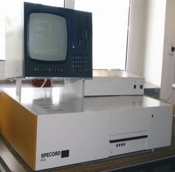 UV-VIS-NIR Spectrophotometer,
SPECORD M42 |
| |
Quality & Reliability Analysis for semiconductor devices
(sensors, microsystems, integrated circuits, transistors, diodes, etc.)
-This service package contains: InceTests (for quality certifying, mechanic-climatic ones, reliability ones); Analyses (failure & reliability ones); Assessment of reliability parameters; Reliability screening; Standardisation documents (standards, workbooks, etc.); Training
courses.
- This is exactly what you need! If you are a manufacturer of
semiconductor devices or a producer of electronic systems (containing semiconductor devices). We offer you the necessary support for
conquering Romanian and foreign markets, because the reliability ("the confidence in product") is the essential parameter for becoming
COMPETITIVE!
- Virtual prototyping. A new concept, developed in IMT, meaning to simulate the reliability of the future product even from the project phase. It is based on a deep knowledge of the models for the degradation phenomena in the elements of the designed product, in the spirit of Concurrent Engineering.
Contact: PhD. Marius Bazu, e-mail: [email protected];
___________________________________ |
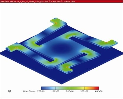 3D model for a moving membrane,
constitutive element of a sensor - a
Fabry-Perrot microcavity. |
| Contact: [email protected] |